210R Silicon Wafer: Enhancing Photovoltaic Efficiency with Rectangular Design
In the global photovoltaic industry's journey towards a more efficient and low-carbon future, technological innovation remains the core driver of progress. Leveraging robust R&D capabilities and keen market insights, Gokin Solar has established the 210R silicon wafer as a key strategic product direction.
So, what breakthrough features does the 210R silicon wafer possess, making it a critical choice in the industry's size evolution?
I. What is the 210R Silicon Wafer?
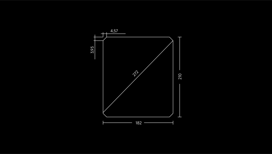
The 210R monocrystalline silicon wafer features a standard size of 210mm (long side) × 182mm (short side). The letter "R" stands for "Rectangle," distinguishing it from traditional square wafers. The rectangular design achieves optimized balance across multiple dimensions:
The 210mm long side maintains the inherent advantages of large-size wafers.
The 182mm short side ensures compatibility and reliability in module production.
To meet the requirements of different module technologies, the 210R has evolved into various fine-tuned specifications, such as 210mm×182.2mm, 210mm×182.3mm, and 182.3x214mm.

II. Why is the 210R Silicon Wafer the Foundation of "Golden Size" Modules?
1. Breakthrough in Power Output
Leveraging the inherent advantages of the 210mm large-size platform combined with advanced N-type TOPCON technology, 210R modules successfully break through power bottlenecks. With only a slight increase in length, they achieve a power increase of 40W, currently reaching up to 640W.
Specific data shows: cell power increases by 17% compared to the 182.2mm, and module power steadily reaches the 640W platform, delivering higher per-watt power generation profit for power plants. (Data source: industry reports)
2. Significant Optimization in Levelized Cost of Electricity (LCOE)
Throughout the manufacturing chain, the 210R demonstrates excellent cost control capabilities. Taking the component production cost at the end of 2024 as an example, the production cost of 210R modules is about 2.88% lower than that of 182.2mm modules and about 5.05% lower than that of 210mm modules. (Data source: industry reports)
This cost advantage stems from:
l Increased power output per unit time.
l Economies of scale from standardized production.
l Significant improvement in material utilization.
3. New Heights in Transportation Efficiency
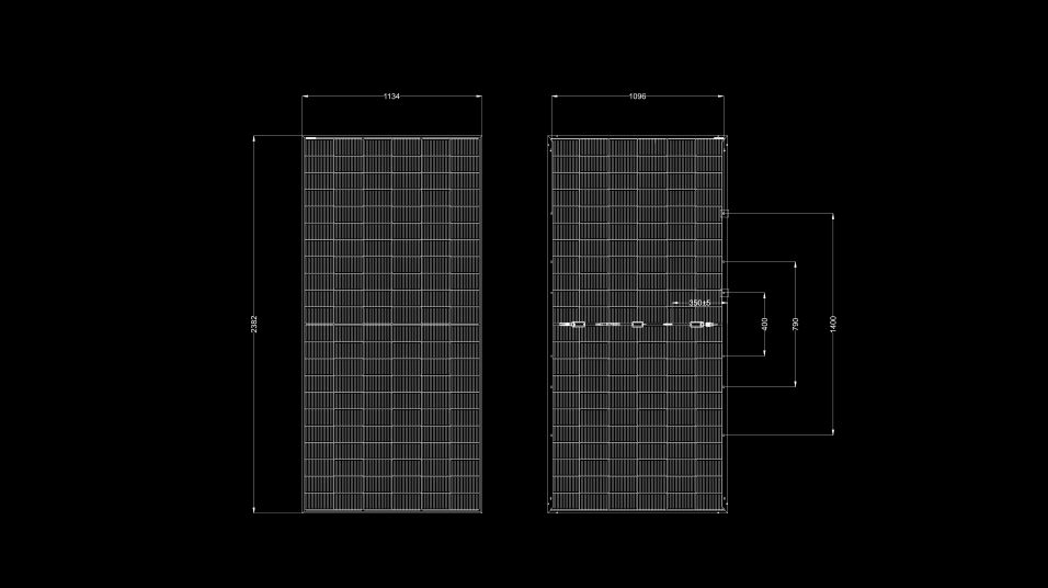
Modules made with N210R silicon wafers typically have overall dimensions of 2382mm in length and 1134mm in width. This "Golden Size" design embodies engineering intelligence. These modules achieve a 98.5% space utilization rate in 40-foot high-cube containers, realizing a "full-capacity" design for container transport and increasing loaded wattage by 5.3%-5.4%. This characteristic significantly reduces shipping costs, providing strong support for overseas market expansion.

4. Promoting Industry Chain Standardization
Before the emergence of N210R, the variety of rectangular wafer sizes (e.g., 183.75mm, 185mm, 186mm) led to complexities in inventory management for upstream wafer and auxiliary material suppliers and poor compatibility in downstream power plant design.
N210R provides the industry with a referenceable, standardized path. Unified dimensions facilitate standardized production for suppliers of wafers, glass, backsheets, frames, and other auxiliary materials, creating economies of scale and reducing costs across the entire industry chain.
III. 210R in Technological Evolution
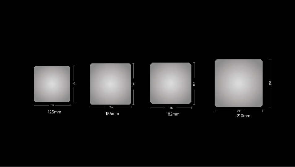
Technological evolution in the photovoltaic industry never ceases. From early 125mm, 156mm to later 182mm, 210mm, size iteration has always been a crucial method for reducing costs and improving efficiency.

As a key rectangular wafer solution at the current stage, 210R is gaining adoption by more companies. Industry data indicates that the market share of the 210 series products is expected to reach 58.4% in 2025, making them mainstream. With accelerated industry adoption, several leading companies have achieved mass production of 210R modules, and their market share is projected to continue rising, exceeding 90% by 2029.
However, we fully understand that there are no eternal size standards in the PV industry, only continuously evolving technological solutions. Whether 210R remains a long-term mainstream choice will ultimately be determined by the efficiency of industry chain collaboration and the value delivered to customers.
In today's era of rapid PV technological iteration, 210R might be just one wave in the long river of industry development. But it teaches us a lesson: true innovation lies not in the size itself, but in how to use wisdom to create tangible value for customers within a specific technological stage.
This is the philosophy Gokin Solar always adheres to – no matter how technology evolves, meeting customer needs and the relentless pursuit of "Perfection" in quality will never become outdated.
210R Silicon Wafer: Advancing Photovoltaic Efficiency with a Rectangular Design
As the global photovoltaic industry continues its transition towards higher efficiency and lower carbon emissions, technological innovation remains the essential driver of progress. Drawing on strong research and development capabilities and deep insight into market trends, Gokin Solar has positioned the 210R silicon wafer as a key strategic product for the next stage of industry development.
So, what makes the 210R silicon wafer a pivotal choice in the evolution of PV wafer sizing?
I. What is the 210R Silicon Wafer?
The 210R monocrystalline silicon wafer features a standard size of 210 mm (long side) × 182 mm (short side). The “R” denotes “Rectangle”, distinguishing it from traditional square wafers. This rectangular design delivers a well-balanced combination of performance and manufacturing benefits:
· The 210 mm long side retains the inherent advantages of large-format wafers.
· The 182 mm short side ensures compatibility and reliability in module assembly.
To support a range of module technologies, the 210R is available in several refined specifications, including 210 mm × 182.2 mm, 210 mm × 182.3 mm, and 182.3 mm × 214 mm.
II. Why is the 210R the Foundation of the Industry’s “Golden Size” Module?
1. Higher Power Output
By combining the 210 mm large-size platform with advanced N-type TOPCon cell technology, 210R-based modules achieve a significant increase in power output. With only a modest increase in module length, power can be raised by approximately 40 W, with module output currently reaching up to 640 W.
Industry data indicates:
· Cell output increases by around 17% compared with 182.2 mm wafers.
· Module power reliably achieves the 640 W range, offering higher power generation efficiency and improved value per watt for utility-scale projects.
2. Lower Levelised Cost of Electricity (LCOE)
Across the manufacturing chain, 210R wafers demonstrate strong cost-efficiency advantages. By the end of 2024, the production cost of 210R modules is expected to be:
· ~2.88% lower than 182.2 mm module production
· ~5.05% lower than conventional 210 mm module production
(Source: industry reports)
These savings are driven by:
· Higher output per unit production time
· Standardised, scalable mass production
· Improved utilisation of raw materials
3. Optimised Transportation Efficiency
Modules using N210R wafers typically measure 2382 mm × 1134 mm. This intelligent “Golden Size” achieves up to 98.5% container space utilisation in 40-foot high-cube containers, increasing shipped wattage by 5.3%–5.4%.
This results in lower logistics costs and enhances competitiveness in overseas markets.
4. Supporting Industry Standardisation
Before the introduction of the 210R, a variety of rectangular wafer formats (e.g., 183.75 mm, 185 mm, 186 mm) created inconsistencies across the supply chain and design limitations downstream.
The N210R provides a unified and referenceable standard, enabling:
· Greater compatibility across materials
· More predictable production planning
· Cost reductions across the entire industry chain
III. 210R in the Context of Technological Evolution
The photovoltaic industry has consistently advanced wafer dimensions — from 125 mm to 156 mm, then 182 mm and 210 mm — as part of its ongoing effort to reduce costs and improve efficiency.
Today, the 210R stands as the most promising rectangular wafer solution. Market forecasts project that 210-series products will reach a 58.4% market share in 2025, becoming mainstream. With increasing adoption, major manufacturers have already achieved large-scale production of 210R modules, with market penetration expected to exceed 90% by 2029.
However, no wafer size remains dominant permanently. The long-term viability of the 210R will ultimately depend on the efficiency of industry collaboration and the real value delivered to customers.
In a period of rapid technological change, the 210R is more than a product — it is a demonstration of principle: innovation matters only when it creates meaningful and measurable value.
This is the philosophy that Gokin Solar upholds — as technology evolves, meeting customer needs and maintaining an unwavering commitment to quality will always remain essential.


